- 您现在的位置:买卖IC网 > Sheet目录317 > C8051F380-TB (Silicon Laboratories Inc)DEV KIT FOR C8051F38X
�� �
�
�C8051F380/1/2/3/4/5/6/7/C�
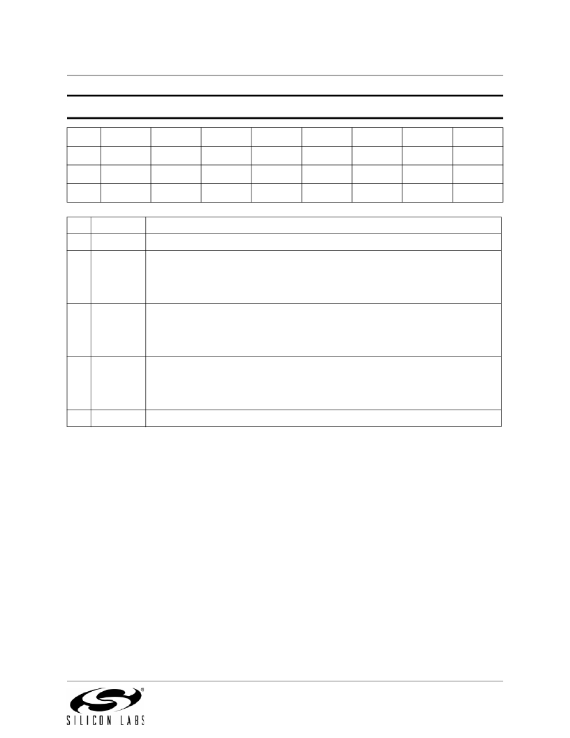
�USB� Register� Definition� 21.19.� EENABLE:� USB0� Endpoint� Enable�
�Bit�
�7�
�6�
�5�
�4�
�3�
�2�
�1�
�0�
�Name�
�EEN3�
�EEN2�
�EEN1�
�Type�
�Reset�
�R�
�1�
�R�
�1�
�R�
�1�
�R�
�1�
�R/W�
�1�
�R/W�
�1�
�R/W�
�1�
�R/W�
�1�
�USB� Register� Address� =� 0x1E�
�Bit� Name�
�Function�
�7:4�
�3�
�2�
�1�
�0�
�Unused�
�EEN3�
�EEN2�
�EEN1�
�Reserved�
�Read� =� 1111b.� Write� =� don’t� care.�
�Endpoint� 3� Enable.�
�This� bit� enables/disables� Endpoint� 3.�
�0:� Endpoint� 3� is� disabled� (no� NACK,� ACK,� or� STALL� on� the� USB� network).�
�1:� Endpoint� 3� is� enabled� (normal).�
�Endpoint� 2� Enable.�
�This� bit� enables/disables� Endpoint� 2.�
�0:� Endpoint� 2� is� disabled� (no� NACK,� ACK,� or� STALL� on� the� USB� network).�
�1:� Endpoint� 2� is� enabled� (normal).�
�Endpoint� 1� Enable.�
�This� bit� enables/disables� Endpoint� 1.�
�0:� Endpoint� 1� is� disabled� (no� NACK,� ACK,� or� STALL� on� the� USB� network).�
�1:� Endpoint� 1� is� enabled� (normal).�
�Must� Write� 1b.�
�21.12.� Controlling� Endpoints1-3� IN�
�Endpoints1-3� IN� are� managed� via� USB� registers� EINCSRL� and� EINCSRH.� All� IN� endpoints� can� be� used�
�for� Interrupt,� Bulk,� or� Isochronous� transfers.� Isochronous� (ISO)� mode� is� enabled� by� writing� 1� to� the� ISO� bit�
�in� register� EINCSRH.� Bulk� and� Interrupt� transfers� are� handled� identically� by� hardware.�
�An� Endpoint1-3� IN� interrupt� is� generated� by� any� of� the� following� conditions:�
�1.� An� IN� packet� is� successfully� transferred� to� the� host.�
�2.� Software� writes� 1� to� the� FLUSH� bit� (EINCSRL.3)� when� the� target� FIFO� is� not� empty.�
�3.� Hardware� generates� a� STALL� condition.�
�21.12.1.� Endpoints1-3� IN� Interrupt� or� Bulk� Mode�
�When� the� ISO� bit� (EINCSRH.6)� =� 0� the� target� endpoint� operates� in� Bulk� or� Interrupt� Mode.� Once� an� end-�
�point� has� been� configured� to� operate� in� Bulk/Interrupt� IN� mode� (typically� following� an� Endpoint0� SET_IN-�
�TERFACE� command),� firmware� should� load� an� IN� packet� into� the� endpoint� IN� FIFO� and� set� the� INPRDY�
�bit� (EINCSRL.0).� Upon� reception� of� an� IN� token,� hardware� will� transmit� the� data,� clear� the� INPRDY� bit,� and�
�generate� an� interrupt.�
�Writing� 1� to� INPRDY� without� writing� any� data� to� the� endpoint� FIFO� will� cause� a� zero-length� packet� to� be�
�transmitted� upon� reception� of� the� next� IN� token.�
�Rev.� 1.4�
�197�
�发布紧急采购,3分钟左右您将得到回复。
相关PDF资料
C8051F912DK
KIT DEV FOR C8051F91X/C8051F90X
C8051F930-TB
BOARD TARGET/PROTO W/C8051F930
C8051T610DB24
DAUGHTER BOARD T610 24QFN SOCKET
C8051T630DB20
BOARD SOCKET DAUGHTER 20-QFN
CAN-100
BOARD EVAL RS232 100QFP
CANADAPT28
KIT ADAPTER CANDEMOBOARD 28PLCC
CAT24AA01WI-GT3
IC EEPROM SERIAL 1KB I2C 8SOIC
CAT24AA02WI-G
IC EEPROM SERIAL 2KB I2C 8SOIC
相关代理商/技术参数
C8051F381
制造商:SILABS 制造商全称:SILABS 功能描述:USB DRIVER CUSTOMIZATION
C8051F381-GM
功能描述:8位微控制器 -MCU USB-64K-Flash
RoHS:否 制造商:Silicon Labs 核心:8051 处理器系列:C8051F39x 数据总线宽度:8 bit 最大时钟频率:50 MHz 程序存储器大小:16 KB 数据 RAM 大小:1 KB 片上 ADC:Yes 工作电源电压:1.8 V to 3.6 V 工作温度范围:- 40 C to + 105 C 封装 / 箱体:QFN-20 安装风格:SMD/SMT
C8051F381-GMR
功能描述:8位微控制器 -MCU USB-Flash-64k-ADC RoHS:否 制造商:Silicon Labs 核心:8051 处理器系列:C8051F39x 数据总线宽度:8 bit 最大时钟频率:50 MHz 程序存储器大小:16 KB 数据 RAM 大小:1 KB 片上 ADC:Yes 工作电源电压:1.8 V to 3.6 V 工作温度范围:- 40 C to + 105 C 封装 / 箱体:QFN-20 安装风格:SMD/SMT
C8051F381-GQ
功能描述:8位微控制器 -MCU USB-64K-Flash
RoHS:否 制造商:Silicon Labs 核心:8051 处理器系列:C8051F39x 数据总线宽度:8 bit 最大时钟频率:50 MHz 程序存储器大小:16 KB 数据 RAM 大小:1 KB 片上 ADC:Yes 工作电源电压:1.8 V to 3.6 V 工作温度范围:- 40 C to + 105 C 封装 / 箱体:QFN-20 安装风格:SMD/SMT
C8051F381-GQR
功能描述:8位微控制器 -MCU USB-Flash-64k-ADC RoHS:否 制造商:Silicon Labs 核心:8051 处理器系列:C8051F39x 数据总线宽度:8 bit 最大时钟频率:50 MHz 程序存储器大小:16 KB 数据 RAM 大小:1 KB 片上 ADC:Yes 工作电源电压:1.8 V to 3.6 V 工作温度范围:- 40 C to + 105 C 封装 / 箱体:QFN-20 安装风格:SMD/SMT
C8051F382
制造商:SILABS 制造商全称:SILABS 功能描述:USB DRIVER CUSTOMIZATION
C8051F382-GQ
功能描述:8位微控制器 -MCU USB-Flash-32k-ADC
RoHS:否 制造商:Silicon Labs 核心:8051 处理器系列:C8051F39x 数据总线宽度:8 bit 最大时钟频率:50 MHz 程序存储器大小:16 KB 数据 RAM 大小:1 KB 片上 ADC:Yes 工作电源电压:1.8 V to 3.6 V 工作温度范围:- 40 C to + 105 C 封装 / 箱体:QFN-20 安装风格:SMD/SMT
C8051F382-GQR
功能描述:8位微控制器 -MCU USB-Flash-32k-ADC RoHS:否 制造商:Silicon Labs 核心:8051 处理器系列:C8051F39x 数据总线宽度:8 bit 最大时钟频率:50 MHz 程序存储器大小:16 KB 数据 RAM 大小:1 KB 片上 ADC:Yes 工作电源电压:1.8 V to 3.6 V 工作温度范围:- 40 C to + 105 C 封装 / 箱体:QFN-20 安装风格:SMD/SMT